


Introduction
The semiconductor industry, long governed by Moore’s Law and incremental improvements in silicon-based technologies, is entering a transformative era. As conventional scaling approaches physical limits, emerging technologies promise to redefine computation, energy efficiency, and device functionality. Researchers and companies are exploring innovations such as quantum computing chips, AI accelerators, neuromorphic architectures, advanced 3D integration, photonic circuits, and two-dimensional materials.
This article delves into these emerging technologies, highlighting their scientific principles, engineering challenges, potential applications, and implications for the future of computing. By examining cutting-edge research and industrial developments, we can glimpse the next generation of semiconductors and understand how they may reshape technology and society.
1. Quantum Computing Chips
Quantum computing represents a paradigm shift in computation, leveraging the principles of quantum mechanics to perform operations that are infeasible for classical computers.
1.1 Qubits: The Fundamental Unit
- Superposition: Qubits can exist in multiple states simultaneously, enabling parallel computation.
- Entanglement: Qubits can be correlated across distances, allowing complex computations through collective interactions.
- Coherence and Decoherence: Maintaining quantum states long enough for computation is a key engineering challenge.
1.2 Types of Quantum Chips
- Superconducting Qubits: Used by companies like IBM and Google. Operate at cryogenic temperatures using Josephson junctions.
- Trapped Ion Qubits: Individual ions confined in electromagnetic traps, manipulated with lasers (e.g., IonQ).
- Topological Qubits: Explored by Microsoft, leveraging exotic quasi-particles to enhance error resistance.
1.3 Engineering Challenges
- Cryogenic Operation: Quantum chips require near-absolute-zero temperatures, complicating integration with classical systems.
- Error Correction: Quantum error correction is essential for reliable computation, requiring hundreds or thousands of physical qubits per logical qubit.
- Scaling: Moving from tens to thousands of qubits while maintaining coherence is a monumental engineering task.
1.4 Potential Applications
- Cryptography: Breaking classical encryption and developing quantum-safe algorithms.
- Drug Discovery: Simulating molecular interactions with unprecedented accuracy.
- Optimization Problems: Logistics, finance, and AI could benefit from quantum-enhanced optimization.
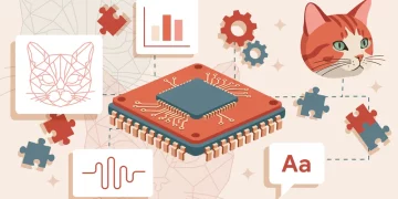
2. AI Accelerators and Specialized Chips
Artificial intelligence has driven demand for specialized hardware optimized for machine learning workloads.
2.1 GPUs and TPUs
- GPUs: Originally designed for graphics, now widely used for deep learning due to massive parallelism.
- TPUs (Tensor Processing Units): Custom ASICs developed by Google, optimized for matrix multiplication and neural network inference.
2.2 Edge AI Chips
- Low-Power Inference: Chips designed for edge devices, balancing computation, energy efficiency, and latency.
- Applications: Autonomous vehicles, smartphones, IoT sensors, and wearable devices.
2.3 Neuromorphic Chips
- Brain-Inspired Architecture: Emulates neurons and synapses to perform massively parallel, event-driven computation.
- Examples: Intel’s Loihi, IBM’s TrueNorth.
- Advantages: Energy-efficient AI processing, particularly for sensory data like vision and auditory signals.
3. Advanced 3D Integration and Chiplets
3.1 Limitations of 2D Scaling
- As transistors shrink below 5 nm, traditional planar scaling faces quantum tunneling, variability, and heat dissipation issues.
- Interconnect delays increasingly dominate performance.
3.2 3D Stacking
- Through-Silicon Vias (TSVs): Vertical electrical connections between stacked dies reduce latency and increase bandwidth.
- Heterogeneous Integration: Combines logic, memory, analog, and photonics in a single package.
- Benefits: Higher performance, smaller form factor, improved power efficiency.
3.3 Chiplet Architectures
- Modular Design: Combines smaller, specialized dies instead of a single monolithic die.
- Flexibility: Allows mixing of mature and advanced nodes, reducing costs and improving yield.
- Examples: AMD’s EPYC processors, Intel’s Foveros technology.
4. Photonics and Optical Interconnects
4.1 The Limits of Electrical Interconnects
- Electrical signals face resistance, capacitance, and signal integrity issues at high frequencies.
- Data centers and high-performance computing require faster and more energy-efficient communication.
4.2 Silicon Photonics
- Integration of Light and Electronics: Uses silicon waveguides, modulators, and detectors on-chip to transmit optical signals.
- Advantages: High bandwidth, low latency, reduced power consumption.
- Applications: Data centers, AI accelerators, high-speed networking.
4.3 Challenges
- Efficient integration with electronic transistors.
- Cost and manufacturability of large-scale silicon photonics systems.
5. Emerging Materials and Device Concepts
5.1 Two-Dimensional (2D) Materials
- Graphene: Exceptional electron mobility, thermal conductivity, and mechanical strength.
- Transition Metal Dichalcogenides (TMDs): MoS2, WS2, and others enable atomically thin transistors.
- Applications: Ultrafast transistors, flexible electronics, transparent displays.
5.2 Spintronics
- Concept: Uses electron spin in addition to charge to encode information.
- Benefits: Non-volatile memory, low-power logic, potentially faster data processing.
- Examples: MRAM (Magnetoresistive RAM), spin-based logic devices.
5.3 Topological Insulators
- Principle: Conduct electricity only on the surface while insulating in the bulk.
- Applications: Robust quantum computing qubits, low-dissipation interconnects.
6. Energy Efficiency and Sustainability
As chip complexity grows, energy consumption has become a critical concern:
- Data Centers: Account for significant global electricity usage, much of it driven by high-performance processors.
- Low-Power Design: AI accelerators and edge chips focus on energy-efficient computation.
- Material Considerations: Advanced semiconductors like GaN and SiC enable more efficient power conversion in EVs and renewable energy.
- Circular Economy: Recycling rare metals from semiconductor manufacturing reduces environmental impact.
7. Industry and Research Landscape
7.1 Leading Innovators
- Tech Giants: Google, NVIDIA, Intel, AMD, IBM, Apple.
- Research Institutions: MIT, Stanford, UC Berkeley, EPFL, Tsinghua University.
- Startups: Quantum computing and neuromorphic startups are driving innovation.
7.2 Collaborative Ecosystems
- Universities, corporations, and government agencies collaborate to develop novel materials, fabrication techniques, and device architectures.
- Public-private initiatives accelerate translation of research into commercial products.
7.3 Funding and Investment Trends
- Venture capital increasingly targets quantum computing, neuromorphic chips, and AI hardware startups.
- Governments provide subsidies, tax incentives, and strategic investments to secure technological leadership.
8. Challenges and Risks
- Manufacturing Complexity: Emerging devices often require exotic materials, cryogenic conditions, or nanoscale precision.
- Economic Barriers: Advanced fabs cost billions; early-stage startups struggle with capital-intensive scaling.
- Talent Shortage: Specialized skills in quantum engineering, photonics, and AI chip design are scarce.
- Standardization: Lack of industry-wide standards for novel architectures complicates adoption.
9. Future Outlook
The semiconductor landscape is poised for a period of rapid transformation:
- Quantum Chips: Will gradually shift from research prototypes to specialized high-value applications.
- AI-Optimized Hardware: Deep learning, edge computing, and real-time inference will drive demand for customized accelerators.
- Neuromorphic Computing: Energy-efficient AI at scale could reshape mobile, IoT, and robotics applications.
- 3D and Chiplet Integration: Modular and stacked architectures will redefine high-performance computing and memory systems.
- Photonics and New Materials: Silicon photonics, graphene, and 2D semiconductors will enable higher speeds and novel functionalities.
These technologies collectively indicate a future where semiconductors are not merely scaled-down silicon devices but diverse, multifunctional, and highly optimized systems tailored for specific computational tasks.
Conclusion
Emerging semiconductor technologies promise to revolutionize computing, communication, and energy efficiency. From quantum computing and AI accelerators to photonic interconnects and neuromorphic chips, the field is moving beyond traditional silicon scaling. These innovations are driven by a combination of scientific breakthroughs, engineering ingenuity, and strategic industrial investments.
While challenges in fabrication, cost, talent, and standardization remain, the potential impact is enormous: enabling faster, smarter, and more energy-efficient technologies that will redefine human interaction with digital systems. For researchers, engineers, and industry leaders, the coming decade represents an unprecedented opportunity to shape the next frontier of semiconductors, pushing the boundaries of what computation and connectivity can achieve.


